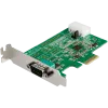
AX99100
PCIe to Multi I/O Controller
Features
PCI Express
Single-lane (X1) PCI Express End-point
Controller with PHY integrated
Compliant with PCI Express 2.0 Gen 1
Compliant with PCI Express card specifications
Compliant with PCI Power Management 1.2
Supports four PCI Express functions
Supports both legacy and MSI Interrupts
Supports ASPM Power Management
Serial Port Interface
Dual or Quad UARTs
Supports RS-232/RS-422/RS-485 multiprotocol
Bi-directional speeds up to 25 Mbps per port
Full Serial Modem Control
Supports Hardware, Software Flow Control
Supports 5, 6, 7, 8 and 9-bit Serial format
Supports Even, Odd, None, Space and Mark parity
Supports Custom baud rate by internal PLL or external clock
Supports On Chip 256 Byte depth FIFOs in
Transmit, Receive path of each Serial Port
Supports remote wakeup and power
management features
Serial Port transceiver shutdown support
Supports Slow IrDA mode (up to 115200bps)
on all Serial Ports
Supports multi-drop application for 9-bit mode
Supports DMA burst transfer
Parallel Port
Compatible with IEEE 1284 – SPP/Byte/ECP Mode
SPI Master Interface
Programmable SPI clock frequency up to 42MHz
Supports Mode 0, Mode 1, Mode 2 and Mode 3 timing modes
Supports MSB/LSB first transfer fashion
Programmable peripheral chip select, selecting up to 7 SPI devices
Supports Non-Burst-Type transfer up to 8 bytes and/or Burst-Type transfer via DMA mode for high performance
Supports to fragment large data block into several
smaller transfers on SPI bus to reduce software loading
Supports programmable transfer 0 ~ 8 bytes
OP-Code field in each transfer automatically to
reduce software loading
Supports wakeup by SWAKEn pin from Slave
Local Bus Interface
Supports memory or I/O access through PCIe
BAR0/1 to local bus interface, each BAR
mapping to local bus' chip select (CS0n and CS1n)
Supports direct access and bus master access (auto-increment and fixed address)
Supports 8-bit or 16-bit data bus width (little and big endian bus swap)
Supports up to 2 Kbytes address space and 2
chip select outputs when separated address/data bus style
Supports up to 64 Kbytes address space and 2 chip select outputs when multiplexed address/data bus style
Supports programmable local chip select region
Supports “Slave Request based DMA” access
for interfacing with external device with bus master
Supports clock out, CLKO, up to 62.5MHz
Supports asynchronous or synchronous Local
Bus with required clock output, CLKO
Supports programmable bus access cycles,
self-terminated bus access cycles and back-to-back turnaround cycles
Supports programmable RSTO, ALE, RDY,
DREQ0/1, DACK0/1, CLKO polarity, and INT0/1 level/edge trigger
Supports wakeup by INT0/1 and DREQ0/1 pins
