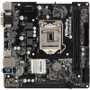
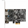
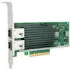
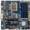
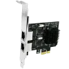
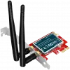
PCI-SIG announced the availability of the PCI Express Base 2.0 specification on 15 January 2007. The PCIe 2.0 standard doubles the transfer rate compared with PCIe 1.0 to 5 GT/s and the per-lane throughput rises from 250 MB/s to 500 MB/s. Consequently, a 32-lane PCIe connector (×32) can support an aggregate throughput of up to 16 GB/s.
PCIe 2.0 motherboard slots are fully backward compatible with PCIe v1.x cards. PCIe 2.0 cards are also generally backward compatible with PCIe 1.x motherboards, using the available bandwidth of PCI Express 1.1. Overall, graphic cards or motherboards designed for v2.0 will work with the other being v1.1 or v1.0a.
The PCI-SIG also said that PCIe 2.0 features improvements to the point-to-point data transfer protocol and its software architecture.
Intel's first PCIe 2.0 capable chipset was the X38 and boards began to ship from various vendors (Abit, Asus, Gigabyte) as of October 21, 2007. AMD started supporting PCIe 2.0 with its AMD 700 chipset series and nVidia started with the MCP72. All of Intel's prior chipsets, including the Intel P35 chipset, supported PCIe 1.1 or 1.0a.
Like 1.x, PCIe 2.0 uses an 8b/10b encoding scheme, therefore delivering, per-lane, an effective 4 Gbit/s max transfer rate from its 5 GT/s raw data rate.
